文章转自ADI官网,版权归属原作者一切
Class D amplifiers, first proposed in 1958, have become increasingly popular in recent years. What are Class D amplifiers? How do they compare with other kinds of amplifiers? Why is Class D of interest for audio? What is needed to make a “good” audio Class D amplifier? What are the features of ADI’s Class D amplifier products? Find the answers to all these questions in the following pages.
Audio Amplifier Background
The goal of audio amplifiers is to reproduce input audio signals at sound-producing output elements, with desired volume and power levels—faithfully, efficiently, and at low distortion. Audio frequencies range from about 20 Hz to 20 kHz, so the amplifier must have good frequency response over this range (less when driving a band-limited speaker, such as a woofer or a tweeter). Power capabilities vary widely depending on the application, from milliwatts in headphones, to a few watts in TV or PC audio, to tens of watts for “mini” home stereos and automotive audio, to hundreds of watts and beyond for more powerful home and commercial sound systems—and to fill theaters or auditoriums with sound.
A straightforward analog implementation of an audio amplifier uses transistors in linear mode to create an output voltage that is a scaled copy of the input voltage. The forward voltage gain is usually high (at least 40 dB). If the forward gain is part of a feedback loop, the overall loop gain will also be high. Feedback is often used because high loop gain improves performance—suppressing distortion caused by nonlinearities in the forward path and reducing power supply noise by increasing the power-supply rejection (PSR).
The Class D Amplifier Advantage
In a conventional transistor amplifier, the output stage contains transistors that supply the instantaneous continuous output current. The many possible implementations for audio systems include Classes A, AB, and B. Compared with Class D designs, the output-stage power dissipation is large in even the most efficient linear output stages. This difference gives Class D significant advantages in many applications because the lower power dissipation produces less heat, saves circuit board space and cost, and extends battery life in portable systems.
Linear Amplifiers, Class D Amplifiers, and Power Dissipation
Linear-amplifier output stages are directly connected to the speaker (in some cases via capacitors). If bipolar junction transistors (BJTs) are used in the output stage, they generally operate in the linear mode, with large collector-emitter voltages. The output stage could also be implemented with MOS transistors, as shown in Figure 1.
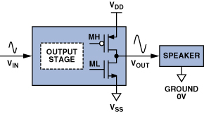
Power is dissipated in all linear output stages, because the process of generating VOUT unavoidably causes nonzero IDS and VDS in at least one output transistor. The amount of power dissipation strongly depends on the method used to bias the output transistors.
The Class A topology uses one of the transistors as a dc current source, capable of supplying the maximum audio current required by the speaker. Good sound quality is possible with the Class A output stage, but power dissipation is excessive because a large dc bias current usually flows in the output-stage transistors (where we do not want it), without being delivered to the speaker (where we do want it).
The Class B topology eliminates the dc bias current and dissipates significantly less power. Its output transistors are individually controlled in a push-pull manner, allowing the MH device to supply positive currents to the speaker, and ML to sink negative currents. This reduces output stage power dissipation, with only signal current conducted through the transistors. The Class B circuit has inferior sound quality, however, due to nonlinear behavior (crossover distortion) when the output current passes through zero and the transistors are changing between the on and off conditions.
Class AB, a hybrid compromise of Classes A and B, uses some dc bias current, but much less than a pure Class A design. The small dc bias current is sufficient to prevent crossover distortion, enabling good sound quality. Power dissipation, although between Class A and Class B limits, is typically closer to Class B. Some control, similar to that of the Class B circuit, is needed to allow the Class AB circuit to supply or sink large output currents.
Unfortunately, even a well-designed class AB amplifier has significant power dissipation, because its midrange output voltages are generally far from either the positive or negative supply rails. The large drain-source voltage drops thus produce significant IDS × VDS instantaneous power dissipation.
Thanks to a different topology (Figure 2), the Class D amplifier dissipates much less power than any of the above. Its output stage switches between the positive and negative power supplies so as to produce a train of voltage pulses. This waveform is benign for power dissipation, because the output transistors have zero current when not switching, and have low VDS when they are conducting current, thus giving smaller IDS × VDS.

Since most audio signals are not pulse trains, a modulator must be included to convert the audio input into pulses. The frequency content of the pulses includes both the desired audio signal and significant high-frequency energy related to the modulation process. A low-pass filter is often inserted between the output stage and the speaker to minimize electromagnetic interference (EMI) and avoid driving the speaker with too much high frequency energy. The filter (Figure 3) needs to be lossless (or nearly so) in order to retain the power-dissipation advantage of the switching output stage. The filter normally uses capacitors and inductors, with the only intentionally dissipative element being the speaker.
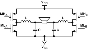
Figure 4 compares ideal output-stage power dissipation (PDISS) for Class A and Class B amplifiers with measured dissipation for the AD1994 Class D amplifier, plotted against power delivered to the speaker (PLOAD), given an audio-frequency sine wave signal. The power numbers are normalized to the power level, PLOAD max, at which the sine is clipped enough to cause 10% total harmonic distortion (THD). The vertical line indicates the PLOAD at which clipping begins.
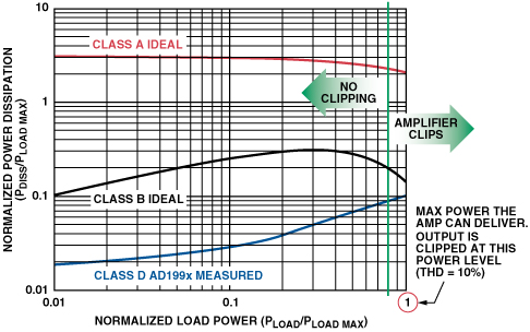
Significant differences in power dissipation are visible for a wide range of loads, especially at high and moderate values. At the onset of clipping, dissipation in the Class D output stage is about 2.5 times less than Class B, and 27 times less than Class A. Note that more power is consumed in the Class A output stage than is delivered to the speaker—a consequence of using the large dc bias current.
Output-stage power efficiency, Eff, is defined as

At the onset of clipping, Eff = 25% for the Class A amplifier, 78.5% for the Class B amplifier, and 90% for the Class D amplifier (see Figure 5). These best-case values for Class A and Class B are the ones often cited in textbooks.
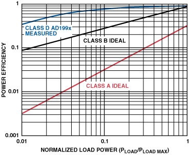
The differences in power dissipation and efficiency widen at moderate power levels. This is important for audio, because long-term average levels for loud music are much lower (by factors of five to 20, depending on the type of music) than the instantaneous peak levels, which approach PLOAD max. Thus, for audio amplifiers, [PLOAD = 0.1 × PLOAD max] is a reasonable average power level at which to evaluate PDISS. At this level, the Class D output-stage dissipation is nine times less than Class B, and 107 times less than Class A.
For an audio amplifier with 10-W PLOAD max, an average PLOAD of 1 W can be considered a realistic listening level. Under this condition, 282 mW is dissipated inside the Class D output stage, vs. 2.53 W for Class B and 30.2 W for Class A. In this case, the Class D efficiency is reduced to 78%—from 90% at higher power. But even 78% is much better than the Class B and Class A efficiencies—28% and 3%, respectively.
These differences have important consequences for system design. For power levels above 1 W, the excessive dissipation of linear output stages requires significant cooling measures to avoid unacceptable heating—typically by using large slabs of metal as heat sinks, or fans to blow air over the amplifier. If the amplifier is implemented as an integrated circuit, a bulky and expensive thermally enhanced package may be needed to facilitate heat transfer. These considerations are onerous in consumer products such as flat-screen TVs, where space is at a premium—or automotive audio, where the trend is toward cramming higher channel counts into a fixed space.
For power levels below 1 W, wasted power can be more of a difficulty than heat generation. If powered from a battery, a linear output stage would drain battery charge faster than a Class D design. In the above example, the Class D output stage consumes 2.8 times less supply current than Class B and 23.6 times less than Class A—resulting in a big difference in the life of batteries used in products like cell phones, PDAs, and MP3 players.
For simplicity, the analysis thus far has focused exclusively on the amplifier output stages. However, when all sources of power dissipation in the amplifier system are considered, linear amplifiers can compare more favorably to Class D amplifiers at low output-power levels. The reason is that the power needed to generate and modulate the switching waveform can be significant at low levels. Thus, the system-wide quiescent dissipation of well-designed low-to-moderate-power Class AB amplifiers can make them competitive with Class D amplifiers. Class D power dissipation is unquestionably superior for the higher output power ranges, though.
Class D Amplifier Terminology, and Differential vs. Single-Ended Versions
Figure 3 shows a differential implementation of the output transistors and LC filter in a Class D amplifier. This H-bridge has two half-bridge switching circuits that supply pulses of opposite polarity to the filter, which comprises two inductors, two capacitors, and the speaker. Each half-bridge contains two output transistors—a high-side transistor (MH) connected to the positive power supply, and a low-side transistor (ML) connected to the negative supply. The diagrams here show high-side pMOS transistors. High-side nMOS transistors are often used to reduce size and capacitance, but special gate-drive techniques are required to control them (Further Reading 1).
Full H-bridge circuits generally run from a single supply (VDD), with ground used for the negative supply terminal (VSS). For a given VDD and VSS, the differential nature of the bridge means that it can deliver twice the output signal and four times the output power of single-ended implementations. Half-bridge circuits can be powered from bipolar power supplies or a single supply, but the single-supply version imposes a potentially harmful dc bias voltage, VDD/2, across the speaker, unless a blocking capacitor is added.
The power supply voltage buses of half-bridge circuits can be “pumped” beyond their nominal values by large inductor currents from the LC filter. The dV/dt of the pumping transient can be limited by adding large decoupling capacitors between VDD and VSS. Full-bridge circuits do not suffer from bus pumping, because inductor current flowing into one of the half-bridges flows out of the other one, creating a local current loop that minimally disturbs the power supplies.
Factors in Audio Class D Amplifier Design
The lower power dissipation provides a strong motivation to use Class D for audio applications, but there are important challenges for the designer. These include:
- Choice of output transistor size
- Output-stage protection
- Sound quality
- Modulation technique
- EMI
- LC filter design
- System cost
Choice of Output Transistor Size
The output transistor size is chosen to optimize power dissipation over a wide range of signal conditions. Ensuring that VDS stays small when conducting large IDS requires the on resistance (RON) of the output transistors to be small (typically 0.1 ohm to 0.2 ohm). But this requires large transistors with significant gate capacitance (CG). The gate-drive circuitry that switches the capacitance consumes power—CV2f, where C is the capacitance, V is the voltage change during charging, and f is the switching frequency. This “switching loss” becomes excessive if the capacitance or frequency is too high, so practical upper limits exist. The choice of transistor size is therefore a trade-off between minimizing IDS × VDS losses during conduction vs. minimizing switching losses. Conductive losses will dominate power dissipation and efficiency at high output power levels, while dissipation is dominated by switching losses at low output levels. Power transistor manufacturers try to minimize the RON × CG product of their devices to reduce overall power dissipation in switching applications, and to provide flexibility in the choice of switching frequency.
Protecting the Output Stage
The output stage must be protected from a number of potentially hazardous conditions:
Overheating: Class D’s output-stage power dissipation, though lower than that of linear amplifiers, can still reach levels that endanger the output transistors if the amplifier is forced to deliver very high power for a long time. To protect against dangerous overheating, temperature-monitoring control circuitry is needed. In simple protection schemes, the output stage is shut off when its temperature, as measured by an on-chip sensor, exceeds a thermal-shutdown safety threshold, and is kept off until it cools down. The sensor can provide additional temperature information, aside from the simple binary indication about whether temperature has exceeded the shutdown threshold. By measuring temperature, the control circuitry can gradually reduce the volume level, reducing power dissipation and keeping temperature well within limits—instead of forcing perceptible periods of silence during thermal-shutdown events.
Excessive current flow in the output transistors: The low on resistance of the output transistors is not a problem if the output stage and speaker terminals are properly connected, but enormous currents can result if these nodes are inadvertently short-circuited to one another, or to the positive or negative power supplies. If unchecked, such currents can damage the transistors or surrounding circuitry. Consequently, current-sensing output-transistor protection circuitry is needed. In simple protection schemes, the output stage is shut off if the output currents exceed a safety threshold. In more sophisticated schemes, the current-sensor output is fed back into the amplifier—seeking to limit the output current to a maximum safe level, while allowing the amplifier to run continuously without shutting down. In these schemes, shutdown can be forced as a last resort if the attempted limiting proves ineffective. Effective current limiters can also keep the amplifier running safely in the presence of momentarily large transient currents due to speaker resonances.
Undervoltage: Most switching output stage circuits work well only if the positive power supply voltages are high enough. Problems result if there is an undervoltage condition, where the supplies are too low. This issue is commonly handled by an undervoltage lockout circuit, which permits the output stages to operate only if the power supply voltages are above an undervoltage-lockout threshold.
Output transistor turn-on timing: The MH and ML output stage transistors (Figure 6) have very low on resistance. It is therefore important to avoid situations in which both MH and ML are on simultaneously, as this would create a low-resistance path from VDD to VSS through the transistors and a large shoot-through current. At best, the transistors will heat up and waste power; at worst, the transistors may be damaged. Break-before-make control of the transistors prevents the shoot-through condition by forcing both transistors off before turning one on. The time intervals in which both transistors are off are called nonoverlap time or dead time.

Sound Quality
Several issues must be addressed to achieve good overall sound quality in Class D amplifiers.
Clicks and pops, which occur when the amplifier is turning on or off can be very annoying. Unfortunately, however, they are easy to introduce into a Class D amplifier unless careful attention is paid to modulator state, output-stage timing, and LC filter state when the amplifier is muted or unmuted.
Signal-to-noise ratio (SNR): To avoid audible hiss from the amplifier noise floor, SNR should typically exceed 90 dB in low-power amplifiers for portable applications, 100 dB for medium-power designs, and 110 dB for high-power designs. This is achievable for a wide variety of amplifier implementations, but individual noise sources must be tracked during amplifier design to ensure a satisfactory overall SNR.
Distortion mechanisms: These include nonlinearities in the modulation technique or modulator implementation—and the dead time used in the output stage to solve the shoot-through current problem.
Information about the audio signal level is generally encoded in the widths of the Class D modulator output pulses. Adding dead time to prevent output stage shoot-through currents introduces a nonlinear timing error, which creates distortion at the speaker in proportion to the timing error in relation to the ideal pulse width. The shortest dead time that avoids shoot-through is often best for minimizing distortion; see Further Reading 2 for a detailed design method to optimize distortion performance of switching output stages.
Other sources of distortion include: mismatch of rise and fall times in the output pulses, mismatch in the timing characteristics for the output transistor gate-drive circuits, and nonlinearities in the components of the LC low-pass filter.
Power-supply rejection (PSR): In the circuit of Figure 2, power-supply noise couples almost directly to the speaker with very little rejection. This occurs because the output-stage transistors connect the power supplies to the low-pass filter through a very low resistance. The filter rejects high-frequency noise, but is designed to pass all audio frequencies, including noise. See Further Reading 3 for a good description of the effect of power-supply noise in single-ended and differential switching output-stage circuits.
If neither distortion nor power-supply issues are addressed, it is difficult to achieve PSR better than 10 dB, or total harmonic distortion (THD) better than 0.1%. Even worse, the THD tends to be the bad-sounding high-order kind.
Fortunately, there are good solutions to these issues. Using feedback with high loop gain (as is done in many linear amplifier designs) helps a lot. Feedback from the LC filter input will greatly improve PSR and attenuate all non-LC-filter distortion mechanisms. LC filter nonlinearities can be attenuated by including the speaker in the feedback loop. Audiophile-grade sound quality with PSR > 60 dB and THD < 0.01% is attainable in well-designed closed-loop Class D amplifiers.
Feedback complicates the amplifier design, however, because loop stability must be addressed (a nontrivial consideration for high-order design). Also, continuous-time analog feedback is necessary to capture important information about pulse timing errors, so the control loop must include analog circuitry to process the feedback signal. In integrated-circuit amplifier implementations, this can add to the die cost.
To minimize IC cost, some vendors prefer to minimize or eliminate analog circuit content. Some products use a digital open-loop modulator, plus an analog-to-digital converter to sense power-supply variations—and adjust the modulator’s behavior to compensate, as proposed in Further Reading 3. This can improve PSR, but will not address any of the distortion problems. Other digital modulators attempt to precompensate for expected output stage timing errors, or correct for modulator nonidealities. This can at least partly address some distortion mechanisms, but not all. Applications that tolerate fairly relaxed sound-quality requirements can be handled by these kinds of open-loop Class D amplifiers, but some form of feedback seems necessary for best audio quality.
Modulation Technique
Class D modulators can be implemented in many ways, supported by a large quantity of related research and intellectual property. This article will only introduce fundamental concepts.
All Class D modulation techniques encode information about the audio signal into a stream of pulses. Generally, the pulse widths are linked to the amplitude of the audio signal, and the spectrum of the pulses includes the desired audio signal plus undesired (but unavoidable) high-frequency content. The total integrated high-frequency power in all schemes is roughly the same, since the total power in the time-domain waveforms is similar, and by Parseval’s theorem, power in the time domain must equal power in the frequency domain. However, the distribution of energy varies widely: in some schemes, there are high energy tones atop a low noise floor, while in other schemes, the energy is shaped so that tones are eliminated but the noise floor is higher.
The most common modulation technique is pulse-width modulation (PWM). Conceptually, PWM compares the input audio signal to a triangular or ramping waveform that runs at a fixed carrier frequency. This creates a stream of pulses at the carrier frequency. Within each period of the carrier, the duty ratio of the PWM pulse is proportional to the amplitude of the audio signal. In the example of Figure 7, the audio input and triangular wave are both centered around 0 V, so that for 0 input, the duty ratio of the output pulses is 50%. For large positive input, it is near 100%, and it is near 0% for large negative input. If the audio amplitude exceeds that of the triangle wave, full modulation occurs, where the pulse train stops switching, and the duty ratio within individual periods is either 0% or 100%.
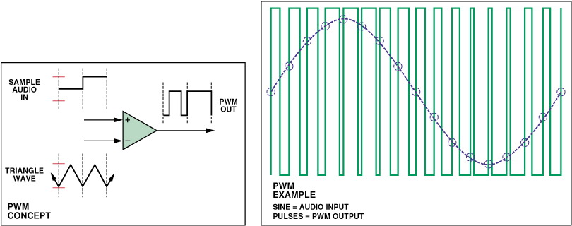
PWM is attractive because it allows 100-dB or better audio-band SNR at PWM carrier frequencies of a few hundred kilohertz—low enough to limit switching losses in the output stage. Also, many PWM modulators are stable up to nearly 100% modulation, in concept permitting high output power—up to the point of overloading. However, PWM has several problems: First, the PWM process inherently adds distortion in many implementations (Further Reading 4); next, harmonics of the PWM carrier frequency produce EMI within the AM radio band; and finally, PWM pulse widths become very small near full modulation. This causes problems in most switching output-stage gate-driver circuits—with their limited drive capability, they cannot switch properly at the excessive speeds needed to reproduce short pulses with widths of a few nanoseconds. Consequently, full modulation is often unattainable in PWM-based amplifiers, limiting maximum achievable output power to something less than the theoretical maximum—which considers only power-supply voltage, transistor on resistance, and speaker impedance.
An alternative to PWM is pulse-density modulation (PDM), in which the number of pulses in a given time window is proportional to the average value of the input audio signal. Individual pulse widths cannot be arbitrary as in PWM, but are instead “quantized” to multiples of the modulator clock period. 1-bit sigma-delta modulation is a form of PDM.
Much of the high-frequency energy in sigma-delta is distributed over a wide range of frequencies—not concentrated in tones at multiples of a carrier frequency, as in PWM—providing sigma-delta modulation with a potential EMI advantage over PWM. Energy still exists at images of the PDM sampling clock frequency; but with typical clock frequencies from 3 MHz to 6 MHz, the images are outside the audio frequency band—and are strongly attenuated by the LC low-pass filter.
Another advantage of sigma-delta is that the minimum pulse width is one sampling-clock period, even for signal conditions approaching full modulation. This eases gate-driver design and allows safe operation to theoretical full power. Nonetheless 1-bit sigma-delta modulation is not often used in Class D amplifiers (Further Reading 4) because conventional 1-bit modulators are only stable to 50% modulation. Also, at least 64× oversampling is needed to achieve sufficient audio-band SNR, so typical output data rates are at least 1 MHz and power efficiency is limited.
Recently, self-oscillating amplifiers have been developed, such as the one in Further Reading 5. This type of amplifier always includes a feedback loop, with properties of the loop determining the switching frequency of the modulator, instead of an externally provided clock. High-frequency energy is often more evenly distributed than in PWM. Excellent audio quality is possible, thanks to the feedback, but the loop is self-oscillating, so it’s difficult to synchronize with any other switching circuits, or to connect to digital audio sources without first converting the digital to analog.
The full-bridge circuit (Figure 3) can use “3-state” modulation to reduce differential EMI. With conventional differential operation, the output polarity of Half-bridge A must be opposite to that of Half-bridge B. only two differential operating states exist: Output A high with Output B low; and A low with B high. Two additional common-mode states exist, however, in which both half-bridge outputs are the same polarity (both high or both low). One of these common-mode states can be used in conjunction with the differential states to produce 3-state modulation where the differential input to the LC filter can be positive, 0, or negative. The 0 state can be used to represent low power levels, instead of switching between the positive and negative state as in a 2-state scheme. Very little differential activity occurs in the LC filter during the 0 state, reducing differential EMI, although actually increasing common-mode EMI. The differential benefit only applies at low power levels, because the positive and negative states must still be used to deliver significant power to the speaker. The varying common-mode voltage level in 3-state modulation schemes presents a design challenge for closed-loop amplifiers.
Taming EMI
The high-frequency components of Class D amplifier outputs merit serious consideration. If not properly understood and managed, these components can generate large amounts of EMI and disrupt operation of other equipment.
Two kinds of EMI are of concern: signals that are radiated into space and those that are conducted via speaker- and power-supply wires. The Class D modulation scheme determines a baseline spectrum of the components of conducted and radiated EMI. However, some board-level design techniques can be used to reduce the EMI emitted by a Class D amplifier, despite its baseline spectrum.
A useful principle is to minimize the area of loops that carry high-frequency currents, since strength of associated EMI is related to loop area and the proximity of loops to other circuits. For example, the entire LC filter (including the speaker wiring) should be laid out as compactly as possible, and kept close to the amplifier. Traces for current drive and return paths should be kept together to minimize loop areas (using twisted pairs for the speaker wires is helpful). Another place to focus is on the large charge transients that occur while switching the gate capacitance of the output-stage transistors. Generally this charge comes from a reservoir capacitance, forming a current loop containing both capacitances. The EMI impact of transients in this loop can be diminished by minimizing the loop area, which means placing the reservoir capacitance as closely as possible to the transistor(s) it charges.
It is sometimes helpful to insert RF chokes in series with the power supplies for the amplifier. Properly placed, they can confine high-frequency transient currents to local loops near the amplifier, instead of being conducted for long distances down the power supply wires.
If gate-drive nonoverlap time is very long, inductive currents from the speaker or LC filter can forward-bias parasitic diodes at the terminals of the output-stage transistors. When the nonoverlap time ends, the bias on the diode is changed from forward to reverse. Large reverse-recovery current spikes can flow before the diode fully turns off, creating a troublesome source of EMI. This problem can be minimized by keeping the nonoverlap time very short (also recommended to minimize distortion of the audio). If the reverse-recovery behavior is still unacceptable, Schottky diodes can be paralleled with the transistor’s parasitic diodes, in order to divert the currents and prevent the parasitic diode from ever turning on. This helps because the metal-semiconductor junctions of Schottky diodes are intrinsically immune to reverse-recovery effects.
LC filters with toroidal inductor cores can minimize stray field lines resulting from amplifier currents. The radiation from the cheaper drum cores can be reduced by shielding, a good compromise between cost and EMI performance—if care is taken to ensure that the shielding doesn’t unacceptably degrade inductor linearity and sound quality at the speaker.
LC Filter Design
To save on cost and board space, most LC filters for Class D amplifiers are second-order, low-pass designs. Figure 3 depicts the differential version of a second-order LC filter. The speaker serves to damp the circuit’s inherent resonance. Although the speaker impedance is sometimes approximated as a simple resistance, the actual impedance is more complex and may include significant reactive components. For best results in filter design, one should always seek to use an accurate speaker model.
A common filter design choice is to aim for the lowest bandwidth for which droop in the filter response at the highest audio frequency of interest is minimized. A typical filter has 40-kHz Butterworth response (to achieve a maximally flat pass band), if droop of less than 1 dB is desired for frequencies up to 20 kHz. The nominal component values in the table give approximate Butterworth response for common speaker impedances and standard L and C values:
| Inductance L (μH) |
Capacitance C (μF) |
Speaker Resistance (Ohm) |
Bandwidth –3-dB (kHz) |
| 10 | 1.2 | 4 | 50 |
| 15 | 1 | 6 | 41 |
| 22 | 0.68 | 8 | 41 |
If the design does not include feedback from the speaker, THD at the speaker will be sensitive to linearity of the LC filter components.
Inductor Design Factors: important factors in designing or selecting the inductor include the core’s current rating and shape, and the winding resistance.
Current rating: The core that is chosen should have a current rating above the highest expected amplifier current. The reason is that many inductor cores will magnetically saturate if current exceeds the current-rating threshold and flux density becomes too high—resulting in unwanted drastic reduction of inductance.
The inductance is formed by wrapping a wire around the core. If there are many turns, the resistance associated with the total wire length is significant. Since this resistance is in series between the half-bridge and the speaker, some of the output power will be dissipated in it. If the resistance is too high, use thicker wire or change the core to a different material that requires fewer turns of wire to give the desired inductance.
Finally, it should not be forgotten that the form of inductor used can affect EMI, as noted above.
System Cost
What are the important factors in the overall cost of an audio system that uses Class D amplifiers? How can we minimize the cost?
The active components of the Class D amplifier are the switching output stage and modulator. This circuitry can be built for roughly the same cost as an analog linear amplifier. The real trade-offs occur when considering other components of the system.
The lower dissipation of Class D saves the cost (and space) of cooling apparatus like heat sinks or fans. A Class D integrated-circuit amplifier may be able to use a smaller and cheaper package than is possible for the linear one. When driven from a digital audio source, analog linear amplifiers require D/A converters (DACs) to convert the audio into analog form. This is also true for analog-input Class D amplifiers, but digital-input types effectively integrate the DAC function.
On the other hand, the principal cost disadvantage of Class D is the LC filter. The components—especially the inductors—occupy board space and add expense. In high-power amplifiers, the overall system cost is still competitive, because LC filter cost is offset by large savings in cooling apparatus. But in cost-sensitive, low-power applications, the inductor expense becomes onerous. In extreme cases, such as cheap amplifiers for cell phones, an amplifier IC can be cheaper than the total LC filter cost. Also, even if the monetary cost is ignored, the board space occupied by the LC filter can be an issue in small form-factor applications.
To address these concerns, the LC filter is sometimes eliminated entirely, to create a filterless amplifier. This saves cost and space, though losing the benefit of low-pass filtering. Without the filter, EMI and high-frequency power dissipation can increase unacceptably—unless the speaker is inductive and kept very close to the amplifier, current-loop areas are minimal, and power levels are kept low. Though often possible in portable applications like cell phones, it is not feasible for higher-power systems such as home stereos.
Another approach is to minimize the number of LC filter components required per audio channel. This can be accomplished by using single-ended half-bridge output stages, which require half the number of Ls and Cs needed for differential, full-bridge circuits. But if the half-bridge requires bipolar power supplies, the expense associated with generating the negative supply may be prohibitive, unless a negative supply is already present for some other purpose—or the amplifier has enough audio channels, to amortize the cost of the negative supply. Alternatively, the half-bridge could be powered from a single supply, but this reduces output power and often requires a large dc blocking capacitor.
Analog Devices Class D Amplifiers
All of the design challenges just discussed can add up to a rather demanding project. To save time for the designer, Analog Devices offers a variety of Class D amplifier integrated circuits, incorporating programmable-gain amplifiers, modulators, and power output stages. To simplify evaluation, demonstration boards are available for each amplifier type to simplify evaluation. The PCB layout and bill-of-materials for each of these boards serve as a workable reference design, helping customers quickly design working, cost-effective audio systems without having to “reinvent the wheel” to solve the major Class D amplifier design challenges.
Consider, for example, the AD1990, AD1992, and AD1994—a family of dual-amplifier ICs, targeted at moderate-power stereo or mono applications requiring two channels with output-per-channel of up to 5-, 10-, and 25-W, respectively. Here are some properties of these ICs:
The AD1994 Class D audio power amplifier combines two programmable-gain amplifiers, two sigma-delta modulators, and two power-output stages to drive full H-bridge-tied loads in home theater-, automotive-, and PC audio applications. It generates switching waveforms that can drive stereo speakers at up to 25 W per speaker, or a single speaker to 50 W monophonic, with 90% efficiency. Its single-ended inputs are applied to a programmable-gain amplifier (PGA) with gains settable to 0-, 6-, 12-, and 18 dB, to handle low-level signals.
The device has integrated protection against output-stage hazards of overheating, overcurrent, and shoot-through current. There are minimal clicks and pops associated with muting, thanks to special timing control, soft start, and dc offset calibration. Specifications include 0.001% THD, 105-dB dynamic range, and >60 dB PSR, using continuous-time analog feedback from the switching output stage and optimized output stage gate drive. Its 1-bit sigma-delta modulator is especially enhanced for the Class D application to achieve average data frequency of 500 kHz, with high loop gain to 90% modulation, and stability to full modulation. A standalone modulator mode allows it to drive external FETs for higher output power.
It uses a 5-V supply for the PGA, modulator, and digital logic, and a high-voltage supply from 8 V to 20 V for the switching output stage. The associated reference design meets FCC Class B EMI requirements. When driving 6 ohm loads with 5-V and 12-V supplies, the AD1994 dissipates 487 mW quiescently, 710 mW at the 2 × 1-W output level, and 0.27 mW in power-down mode. Available in a 64-lead LFCSP package, it is specified from –40°C to +85°C
More technical information about Class D amplifiers—including implementations with Blackfin processors—can be found in the Further Reading section.
Acknowledgements
The author would like to thank Art Kalb and Rajeev Morajkar of Analog Devices for their thoughtful inputs to this article.
Further Reading
- International Rectifier, Application Note AN-978, “HV Floating MOS-Gate Driver ICs.”
- Nyboe, F., et al, “Time Domain Analysis of Open-Loop Distortion in Class D Amplifier Output Stages,” presented at the AES 27th International Conference, Copenhagen, Denmark, September 2005.
- Zhang, L., et al, “Real-Time Power Supply Compensation for Noise-Shaped Class D Amplifier,” Presented at the 117th AES Convention, San Francisco, CA, October 2004.
- Nielsen, K., “A Review and Comparison of Pulse-Width Modulation (PWM) Methods for Analog and Digital Input Switching Power Amplifiers,” Presented at the 102nd AES Convention, Munich, Germany, March 1997.
- Putzeys, B., “Simple Self-Oscillating Class D Amplifier with Full Output Filter Control,” Presented at the 118th AES Convention, Barcelona, Spain, May 2005.
- Gaalaas, E., et al, “Integrated Stereo Delta-Sigma Class D Amplifier,” IEEE J. Solid-State Circuits, vol. 40, no. 12, December 2005, pp. 2388-2397. about the AD199x Modulator.
- Morrow, P., et al, “A 20-W Stereo Class D Audio Output Stage in 0.6 mm BCDMOS Technology,” IEEE J. Solid-State Circuits, vol. 39, no. 11, November 2004, pp. 1948-1958. about the AD199x Switching Output Stage.
- PWM and Class-D Amplifiers with ADSP-BF535 Blackfin® Processors, Analog Devices Engineer-to-Engineer Note EE-242.


