文章转自ADI官网,版权归属原作者一切
Many systems require fixed or programmable digital clock waveforms. In applications where PCB area is constrained, the microcontroller typically generates these signals. Three methods for generating a clock using an ADuC702x Analog Microcontroller are presented here.
A classic solution for clock generation is to toggle one of the microcontroller’s general-purpose outputs. If a timer is available, it can be configured to complement the general-purpose output in the interrupt service routine, each time it overflows. This type of fully programmable digital waveform generation allows for a programmable duty cycle, but the interrupt latency limits its speed and precision. The ARM7 based ADuC702x has a variable interrupt latency. This variation creates jitter on the generated signal. Another liability of this method is that the timer interrupt has to be serviced with high priority in order to maintain correct timing. Ideally, the digital waveform generation shouldn’t involve the core.
One solution that doesn’t involve the core uses an integrated PWM (pulse-width modulator). This method also allows variable duty cycles. The clock resolution depends on the size of the PWM switching frequency register and core clock frequency. The main advantages of this solution are that there is no CPU load, and that a wide range of frequencies can be generated—from a few hertz to tens of megahertz. The ADuC702x family integrates a PWM block, as shown in figure 1.
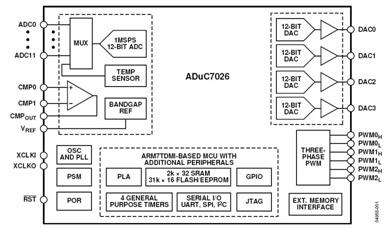
The disadvantages of this solution are that the precision of the PWM generated clock is dependant of the precision of the internal clock, and that it uses a full 3-phase PWM block that was not intended originally for this purpose. The accuracy can be improved by using an external 32 kHz crystal instead of the ±3% accurate on-chip oscillator, but this adds to the cost, size, and power budgets.
A smaller solution consists in using a gate and flip flop. The ADuC702x family includes a programmable logic array (PLA) that can be used to implement glue logic. This PLA consists of 16 programmable gates and flip-flops that are entirely configurable by software. A very simple clock can be programmed using only a NOT gate and a flip-flop, as show in Figure 2.
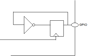
The flip-flop can be clocked from the core clock, the internal 32-kHz oscillator, Timer1, or a general-purpose input. The clock frequency can be very flexible, but the duty cycle cannot be programmed. The big advantage of this solution is that it ties up only a very small block of the chip. The integration of uncommitted gates on the ADuC702x allows great flexibility.
The table below summarizes the characteristics of the three approaches. While each approach has advantages only the application can determine which one is the most appropriate solution.
Table 1: comparison of three methods on the ADuC702x series
| Minimum speed | Maximum speed | Advantages | Disadvantages | |
| GPIO | Using T1: 1/2^32 |
Interrupt latency:
声明:本文内容来自网络转载或用户投稿,文章版权归原作者和原出处所有。文中观点,不代表本站立场。若有侵权请联系本站删除(kf@86ic.com)https://www.86ic.net/changshang/44429.html
|


