文章转自ADI官网,版权归属原作者一切
In systems that utilize feedback, the feedback network is a circuit configured for a particular gain and phase relationship—for example, an adjustable proportional-integral-differential (PID) controller to manipulate the loop gain and/or phase to ensure stability (see Figure 1). It is often desirable to measure the performance of this feedback network in a particular configuration so as to model the open-loop behavior. But this type of measurement is often challenging. For example, the low-frequency gain of an integrator can be very high, generally exceeding the measurement range of conventional test and measurement equipment. The goal of such measurements is to characterize the frequency response of the network rapidly and with minimal effort, using available tools and a small amount of special circuitry.

Q. That makes sense. I have an example of a project that I would welcome suggestions for.
A. Tell me about it.
Q. To qualify a recent design, I had been working on a programmable feedback network and needed to collect hard data to verify the expected behavior. To collect the data, I evaluated the available test equipment and pieced together a crude open-loop measurement system using a general-purpose interface-bus (GPIB) IEEE-488 interfacing card, a simple digital oscilloscope, and an arbitrary function generator (see Figure 2).
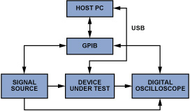
Using the available developer libraries for the GPIB interface, I wrote software to perform data-point collection for Bode plots. In much the same way that we learned in engineering school to draw a Bode plot by hand, the function generator was set to output a sine wave at a set of frequencies, point by point, as the system’s “input.” The oscilloscope then measured both the system input and system output to calculate the gain at a given frequency.
A. How did that turn out?
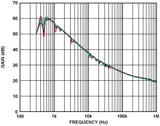
Q. After performing numerous iterations with the devices-under-test, the faults of performing open-loop measurements on a budget, using standard lab equipment, became apparent. High precision required many data points, and each data point consumed significant amounts of time simply to exchange messages between the software and test equipment. The resolution of the oscilloscope also became a factor: at low input amplitudes, noise dominated the system and made triggering difficult. I also observed intermittent rogue samples of data (see Figure 3). Upon investigating, I found that these erroneous samples occurred before the test equipment had finished updating its settings—in effect a system settling-time issue. In the end, each test consumed an incredible 35 minutes. Analyzing the time usage for the test, I found that, for each sample, most of the time was spent in communication between the host and the test equipment, rather than actually performing the measurement.
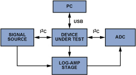
A. Execution time would improve if you were to implement hardware functions to replace software routines. For example, utilizing the available I2C serial bus on your programmable device, less time would be spent sending ASCII characters to form text-based command messages. By making this change, you’re removing several layers of abstraction and interpretation from your test loop, resulting in precise and direct control of the system’s operation.
Q. What hardware devices would it take to implement such a scheme?
A. Use a wideband direct digital synthesizer (DDS) IC, such as the AD5932, to replace the function generator. This DDS provides your design with excellent frequency range and a high-quality sinusoidal output. Gain measurement becomes a simple task with the application of a pair of logarithmic amplifier ICs, such as the AD8307, and a difference amplifier. And the final critical piece of the acquisition system is an analog-to-digital converter IC to replace the digital oscilloscope. Using a multi-input ADC, such as the AD7992 or AD7994, will lower the total cost of the system by using two available channels to capture the logarithmic amplifiers’ result and perform the difference operation in software. The revised arrangement will look like Figure 4.
Q. How does gain measurement with a log amp work?
A. In response to ac inputs, the AD8307 low-cost, easy-to-use logarithmic amplifier produces a dc output—equivalent to 25 mV/dB of input power (0.5 V per decade of voltage) into a 50-ohm load. With a wide dynamic range of 92 dB, the device allows the user to measure even the small input signals experienced in high-gain, open-loop circuits. While you will not actually be driving 50-ohm loads, this standard allows calculating gain (in dB) as the difference of two AD8307 device outputs, which measure the signal input and output.
Q. Can you explain this in more detail?
A. We start with a brief review of logarithm rules:
 |
(1) | |
 |
(2) | |
 |
(3) |
Electrical power gain or attenuation is typically expressed as a log ratio: Since the world of dB deals with ac voltages, VA and VB are rms voltages, and, consequently, PA and PB are average power levels.
 |
(4) |
For unity impedance-ratios, log 1 = 0. Thus, for equal-resistance loads,
 |
(5) |
In high-impedance voltage-amplifier circuits the focus is on signal gain, rather than power gain. So dB is a logarithmic expression of the ratio of output amplitude to input amplitude.
At zero dB, the voltage ratio is unity. To express a given power level measurement in dB, it must be referred to a reference power level. In standard practice, if the measured power is equal to 1 mW, the absolute power level is 0 dBm (or dB above a milliwatt). For a 50-ohm load,
 |
(6) |
Using a low-distortion sine wave, Vrms and average power—for a 50-ohm system—is calculated using Equations 7 and 8:
 |
(7) | |
 |
(8) |
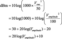
Thus, for 0 dBm, or 1 mW, the input voltage amplitude is 316.2 mV (or 223.6 mV rms). If that is the input level, and the output amplitude of the device under test is 3.162 V (a gain of 10 with an rms amplitude of 2.236 V), then from Equation 6 the output power is +20 dBm, the same as one would obtain from the voltage gain expressed by the ratio in Equation 5. The values are consistent so long as the references are consistent. We can therefore find the system gain easily.
Combining Equation 8 and Equation 6,
 |
(9) |
Apply the log amplifier’s conversion gain of 25mV/dB:
 |
(10) |
Applying Equation 1, using two AD8307 log amplifiers to measure output and input, their difference results in an easy measurement of gain.
 |
(11) |
The AD8307’s inherent output at 0 dB is about 2.0 V. However, the constants (when calibrated) drop out of the equation when the output is calculated as the difference of the log amp outputs.
Q. How do you find the difference?
A. There are many options to obtain the difference, ranging from an easy-to-apply instrumentation amplifier, such as the AD622 or AD627, to a discrete multi-op-amp solution, or even in software after conversion to digital, perhaps using a multichannel ADC like the AD7994. For best accuracy, the designer must, of course, calibrate to eliminate gain- and offset errors between devices. Data sheets available on the Analog Devices website provide this information—as well as excellent tips on frequency-specific issues.
Q. You mentioned the AD5932 direct digital synthesizer. What is that?
A. The AD5932 DDS is a simple, programmable, digitally controlled waveform generator. Using a few simple instructions, the user can configure sine waves, for example, with a complete frequency and phase profile. While this device does not possess an I2C interface, a GPIO device on the I2C bus can perform bit-banging operations to imitate the expected interface. After configuration is completed, a single write to the GPIO device can increment the output frequency.
The output of the AD5932 is 580 mV peak-to-peak, a value that is, in most cases, too large an input for open-loop gain measurement. The attenuation needed depends on the input level appropriate for gain measurement of the device under test at its specified output level. If the input signal is too large, the output will be distorted, or even clipped, giving false measurements. If the signal is too small, offset errors and noise will dominate the waveform’s output and cause problems. A typical signal starts at 10 mV in amplitude, then increases to produce the specified device output value—or the largest value possible without clipping or distortion, as distortion will cause measurement errors.
Q. Can you give me an example of how it works?
A. After assembling the circuit building blocks as shown in Figure 4, you can verify (or calibrate) the performance using, first, a unity-gain amplifier, then a gain-of-10 amplifier in place of the device under test.
Figure 5 is an example of measurements showing unity gain and a gain of 10, actually about 1 dB high, with variation held to well within ±1 dB.
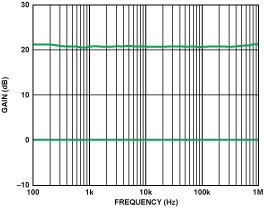
Note the uncalibrated excess gain of +1 dB for the 20-dB setting.
As another example, once confidence in the technique is gained, a sample device with a known behavior can then be tested. Figure 6 shows a typical result, superimposed on the previously collected data to verify the accuracy of this method vs. that of the method you described. The result of the test revealed an error of about ±0.5 dB, indicating that the new system measurement had the same measurement characteristics, but with far lower noise and faster settling times.
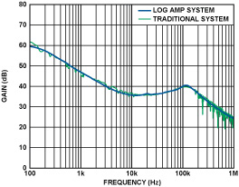
Note the “sampling noise” of the traditional system.
Equipment:
- National Instruments Cardbus GPIB adapter
- Tektronix TDS3032B with GPIB
- Tektronix AFG320 with GPIB
Q. The correlation looks good, and there seem to be none of the outliers plotted in the earlier method. How long did it take to scan through this set of measurements?
A. Each test run was completed in under 35 seconds.
Q. Wow! That’s an improvement of about 6000%.
A. Yes, and, in addition, the simplicity of the design lends itself easily to use in embedded systems, as the majority of the math operations are managed by the log amplifiers. A clever designer could also integrate a phase-measurement device and turn this system into a true Bode-plotter. And you could obtain an all-in-one solution, with high-frequency applications, using the single-chip AD8302 gain- and phase-measuring log amp.


