Freescale Kinetis L Series KL03 MCUs
Freescale did a full market launch of the entire KL03 family, introducing a number of devices and a Freedom board in which customers can get started on their development. The Kinetis KL03 is the ultimate product for portable devices within the IoT space due to its small size and low power consumption (Figure 1). The device also maintains an optimized level of on-chip integration to help customers simplify design and reduce BOM costs and is supported by Freescale’s expansive set of software and tools.

Figure 1: Trends in embedded product design.
The KL03 is in fact smaller than a golf ball dimple (as illustrated by the image in Figure 2), 35% smaller than the nearest competition, but still offers more GPIO than the competition. With a tiny footprint package of 1.6 x 2.0 mm2 WLCSP, the KL03 includes: run power consumption as low as 50 μA/MHz, static power consumption as low as 2.2 μA with 7.5 μs wakeup time for full retention and lowest static mode down to 77 nA in deep sleep, and highly integrated peripherals, including boot ROM and high accurate internal voltage reference.

Figure 2: Kinetis KL03 size comparison.
The KL03 family features include:
A 48 MHz ARM® Cortex®-M0+ core 1.71-3.6 V operation Up to 32 KB flash memory 2 KB RAM 8 KB ROM boot loader for easy flash upgrade Bit manipulation engine for faster, more code-efficient bit-oriented math A high-speed 12-bit analog-to-digital converter Embedded 1.2 V voltage reference for ADC A high-speed analog comparator Low-power UART, SPI, I2C (high speed up to 1 Mb/s) Powerful timers for a broad range of applications, including motor control Operating temperature of -40°C to +105°C QFN (WLCSP is -40°C to +85°C operation) Up to 22 GPIOs, depending on the package
When the customer thinks of Kinetis L, think small size and low power, but also think big portfolio. The Kinetis L series is big and getting bigger. Since introducing this series in September 2012, the portfolio has now grown to more than 200 devices. The LPUART will be provided in more details on each of the different part numbers data sheet. However, the overview table shown in Figure 3 is a good way to see where the KL03 fits in and how to position it with the rest of the devices.
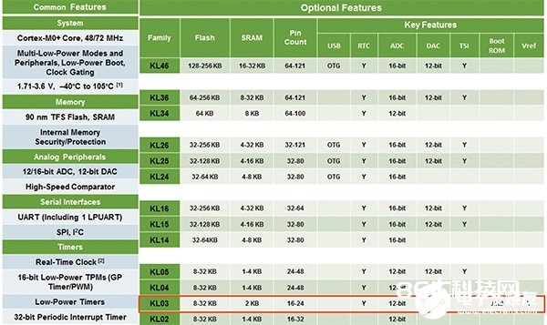
Figure 3: Kinetis L series: MCU families.
As depicted in Figure 4, the Freescale Freedom development platform is a set of software and hardware tools for evaluation and development. It is ideal for rapid prototyping of microcontroller-based applications. The Freescale Freedom KL03Z hardware, FRDM-KL03Z, is a simple, yet sophisticated design featuring a Kinetis L series MCU, built on the ARM Cortex-M0+ core. Processor Expert is a simplified code initialization tool designed to provide 80% of the required firmware from Freescale, allowing designers to focus on the 20% of their own internal code that truly differentiates their products. Solution Advisor is a web-based tool, available on the Freescale website, which allows designers the ability to identify the ideal Kinetis solution by defining the operating characteristics of the device they need, memory configuration, analog, communications and clock peripherals. In addition, it directs them to the associated hardware and software tools and documentation and verifies pin mixing compatibility.
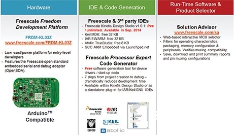
Figure 4: Resources graphic.
In summary, Freescale’s Kinestis L series KL03 is one of the world’s smallest ARM-based MCUs and has excellent performance, is energy-efficient and has many features integrated into a small 1.6 mm x 2.0 mm WLCSP package, enabling miniaturized designs in portable consumer and industrial applications. If the customer is developing a portable application, energy efficiency is going to be a key selling point and with nine low-power modes, this chip has the flexibility to provide power optimization based on the application’s specific requirements. Finally, with software being so much of a customer’s engineering expense today, customers are always looking for ways to reduce their time to market and simplify their software requirements. Using tools, like the Kinetis Design Studio IDE and the Software Development Kit, could save designers months of engineering time and provide them a more seamless way to move around within the ever-expanding Kinetis portfolio, which offers a broad selection of compatible and scalable devices.
飞思卡尔Kinetis L系列MCU KL03
飞思卡尔做了全面的商场推出的整个KL03宗族的,引进了一些设备和一自在板,其客户能够在他们的开展开始运用。所述的Kinetis KL03是对的IoT空间内的便携式设备的终究产品,因为其小尺度和低功耗(图1)。该器材还坚持了片上集成的优化水平协助客户简化规划并下降BOM本钱,并支撑飞思卡尔的胀大一套软件和东西。

图1:在嵌入式产品规划趋势。
该KL03实际上比高尔夫球凹坑(如在图2中所示的图画),比最接近的竞赛小35%以下,但仍供给了比竞赛更多的GPIO。跟着1.6×2.0平方毫米WLCSP小尺度封装,KL03包含:运转功耗低至50μA/ MHz的,静态功耗低至2.2μA7.5微秒的唤醒时刻充沛保存和最低的静态形式下为77娜深度睡觉,并高度集成的外设,包含引导ROM和高准确的内部电压基准。
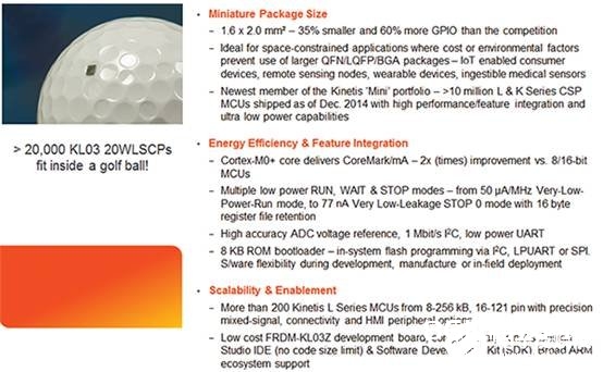
图2:的Kinetis KL03巨细比较。
该KL03系列的特性包含:
•48 MHz的ARM®Cortex®-M0 +内核
•1.71-3.6 V作业
•高达32 KB的Flash存储器
•2 KB RAM
便利的闪存晋级•8 KB的ROM引导装载程序
•位操作引擎更快,更多的代码功率面向比特的数学
•一个高速12位模仿数字转换器
•用于嵌入式ADC 1.2 V基准电压
•一个高速模仿比较器
•低功耗UART,SPI,I2C(高速可达1 Mb / s的)
•强壮的定时器,用于广泛的运用,包含电机操控
•作业在-40°C的温度至+ 105°C QFN封装(WLCSP为-40°C至+ 85°C的操作)
•多达22个GPIO,取决于包
当客户想到的Kinetis L,以为小尺度和低功耗,并且还觉得大组合。该的Kinetis L系列是大而变得越来越大。自从推出这个系列的2012年9月,出资组合,现在现已开展到超越200台设备。该LPUART将在每个不同的部件号数据表的更多细节来供给。但是,在图3所示的概述表上看到KL03合适于和怎么将其与设备的其余部分的方位的杰出途径。
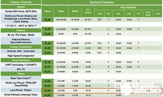
图3:的Kinetis L系列:MCU系列。
如描绘在图4中,飞思卡尔自在开发渠道是一组用于评价和开发的软件和硬件东西。它是十分合适根据微操控器的运用的快速原型规划。飞思卡尔自在KL03Z硬件,FRDM-KL03Z,是一种简略,但杂乱的规划,具有的Kinetis L系列MCU,内置于ARM的Cortex-M0 +内核。处理器专家是一个简化的代码初始化东西,旨在供给80%来自飞思卡尔所需的固件,使规划人员能够专心于自己的内部代码的20%,真实区别他们的产品。解决方案参谋是一个根据Web的东西,可在飞思卡尔的网站,它答应规划人员经过界说自己所需求的设备,内存装备,模仿,通讯和时钟外设的作业特性来确认抱负的Kinetis解决方案的才能上。此外,它指示它们相关的硬件和软件东西和文档,并验证销混合相容性。

图4:资源的图形。
总归,飞思卡尔的Kinestis L系列KL03是世界上最小的根据ARM的微操控器之一,具有优异的功用,是节能的,并具有许多功用集成到一个小型1.6毫米×2.0毫米WLCSP封装,在便携式消费完成小型化规划和工业运用。假如客户正在开发一种便携式的运用程序,能效将是一个要害的卖点,并与九个低功耗形式,该芯片具有很大的灵活性,以供给根据运用程序的具体要求来优化功耗。最终,软件这么多的今日客户的工程费用,客户一直在寻觅办法,以削减他们的上市时刻并简化其软件需求。运用的东西,像Kinetis产品规划作业室IDE和软件开发东西包,能够节约工程时刻规划个月,并为他们供给愈加无缝的方法来不断扩大的Kinetis组合中走动,它供给了一个宽广的挑选兼容的,可扩展的设备。


