latTIce公司的iCE40 HX超低功耗mobileFPGA系列,和其它任何的CPLD或FPGA器材比较,可提供最低的静态和动态功耗,大约640到7680个逻辑单元和触发器,每个器材包括8到32个RAM区块,每个区块有4Kb存储,用于数据存储和缓冲,特别合适对本钱灵敏和量大的使用。本文介绍了iCE40 HX系列首要特性,iCE40 HX系列架构图,首要产品和特性,以及iCEblink40 iCE40HX1K 评价板首要特性,电路图,首要元件清单和PCB元件布局图。
The LatTIce Semiconductor iCE40 LP-Series and HX-Series programmable logic family are designed to deliver the lowest staTIc and dynamic power consumpTIon of any comparable CPLD or FPGA device. iCE40 FPGAs are designed specifically for cost-sensitive, high-volume applications. iCE40 FPGA are fully user-programmable and can self-configure from a configuration image stored in on-chip, nonvolatile configuration memory (NVCM) or stored in an external commodity SPI serial Flash PROM or downloaded from an external processor over an SPI-like serial port. iCE40 components deliver from approximately 640 to 7,680 logic cells and flip-flops while consuming a fraction of the power of comparable programmable logic devices. Each iCE40 device includes 8 to 32 RAM blocks, each with 4Kbits storage, for on-chip data storage and data buffering.
Each iCE40 device consists of five primary architectural elements.
An array of Programmable Logic Blocks (PLBs)
Each PLB contains eight Logic Cells (LCs); each Logic Cell consists of …
A fast, four-input look-up table (LUT4) capable of implementing any combinational logic function of up to four inputs, regardless of complexity
A‘D’-type flip-flop with an optional clock-enable and set/reset control
Fast carry logic accelerates arithmetic functions: adders, subtracters, comparators, and counters.
Common clock input with polarity control, clock-enable input, and optional set/reset control input to the PLB is shared among all eight Logic Cells
Two-port, 4Kbit RAM blocks (RAM4K)
256×16 default configuration; selectable data width using programmable logic resources
Simultaneous read and write access; ideal for FIFO memory and data buffering applications
RAM contents pre-loadable during configuration
Four I/O banks with independent supply voltage, multiple Programmable Input/Output (PIO) blocks
LVCMOS I/O standards and LVDS outputs supported in all banks
I/O Bank 3 supports additional LVDS, and SubLVDS I/O standards
One or two Phase-Locked Loops (PLL)
Very low power
Clock multiplication and division
Phase shifting in fixed 90° increments
Static or dynamic phase shifting
Programmable interconnections between all programmable logic functions
Eight dedicated low-skew, high-fanout clock distribution networks
iCE40 HX系列首要特性:
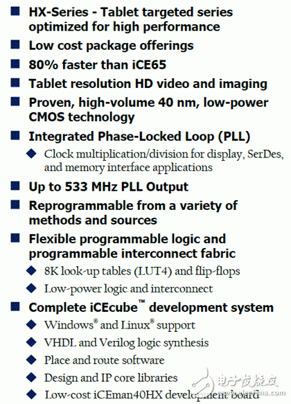
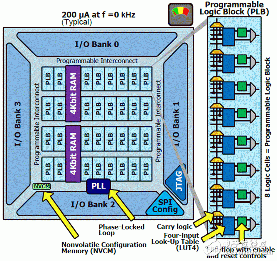
图1.iCE40 HX系列架构图和特性
iCE40 HX超低功耗可编程逻辑系列首要产品和特性:
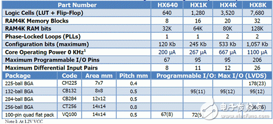
The HX-Series of the iCE40™ “Los Angeles” mobileFPGA™ family is ideal for tablet applications.
Designers of handheld, battery-based consumer products have long awaited a programmable logic solution that delivers design flexibility and fast time-to-market benefits coupled with features that address their power, logic capacity, cost, and small form factor requirements. This solution, previously unattainable by other FPGA suppliers, is now provided by Lattice’s ultra-low power mobileFPGA devices.
Utilizing the mobileFPGA platform, mobile designers can quickly bring new features and custom functionality to market with their very own Custom Mobile Device. Designers can achieve this by either using state of the art development software or by utilizing Lattice’s design services.
Key Features
Ideal for sensor management functions including interrupt filtering, interrupt aggregation, auto polling
Battery insertion and audio insertion detection with high speed comparators
Support MIPI SLIMbus Interface
High speed LVDS channels up to 525 Mbps per channel
High definition video support: HD720p @ 60Hz, HD1080p @ 30Hz
Supports MIPI DBI and MIPI DPI video interface standards
High Speed USB 2.0 host and device controllers supporting ULPI and UTMI interfaces Ideal for 3D solutions
PCB friendly footprint packages
Fabricated on advanced 40nm standard CMOS process
50% faster than iCE65™ devices
Ultra-low power consumption
Ultra-small footprint packages
World’s first 2.5 x 2.5 mm, 0.4mm pitch ball grid array
2X logic capacity per mm2 over iCE65
Up to 2 phase-locked loops supporting dual outputs
Flexible block RAM
iCEblink40 iCE40HX1K 评价板
This guide describes how to begin using the iCEblink40 Evaluation Kit, an easy-to-use platform for rapidly prototyp-ing designs using the iCE40 mobileFPGA™。
iCEblink40 iCE40HX1K 评价板首要特性:
• High-performance, low-power iCE40HX1K mobileFPGA
• USB programming, debugging, virtual I/O functions, and power supply
• Four user LEDs
• Four capacitive-touch buttons
• 3.3 MHz clock source
• 1Mbit SPI serial configuration PROM
• Supported by Lattice iCEcube2™ design software
• 68 LVCMOS/LVTTL (3.3V) digital I/O connections on 0.1” through-hole connections
• Supports third-party I/O expansion boards and modules, including 3.3V Arduino Shield boards (requires additional sockets, not supplied)
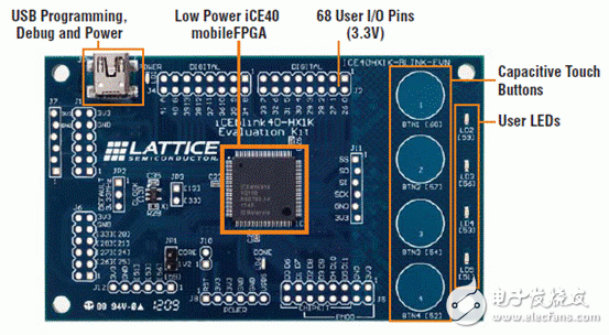
图2.iCEblink40 iCE40HX1K 评价板外形图
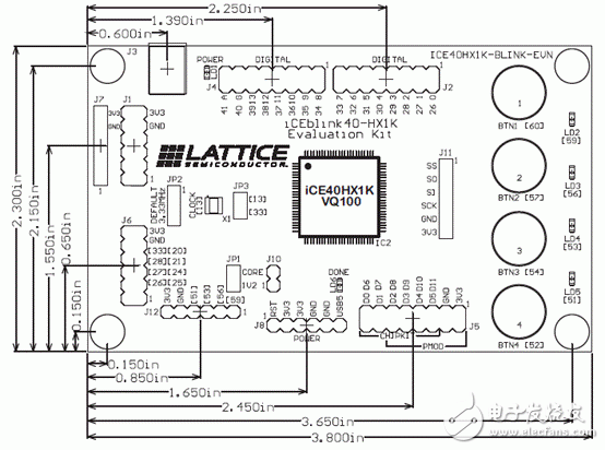
图3.iCEblink40 HX1K评价板元件布局图和板尺度
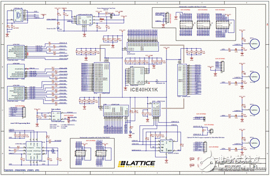
图4.iCEblink40 iCE40HX1K评价板电路图


