文章转自ADI官网,版权归属原作者一切
Introduction
Switch-mode power supplies are used throughout modern electronics systems mainly because of their high efficiency power conversion. One side effect of the proliferation of switch-mode supplies is the noise they produce. This is commonly referred to as electromagnetic interference (EMI), EMI noise, or just noise. For example, the input side switch current of a typical buck converter is a pulsating current rich in harmonic content. Fast turn-on and turn-off of power transistors create sudden interruptions of current flow, resulting in high frequency voltage ringing and spikes.
The problem is that high frequency noise can couple to other devices in the system, degrading the performance of sensitive analog or digital signal circuits. Because of this, many standards have arisen to set acceptable limits on EMI. To meet these limits for a switch-mode supply, one must first quantify its EMI performance and, if necessary, add proper input EMI filtering to attenuate the EMI. Unfortunately, EMI analysis and filter design can be a difficult task, typically requiring a time-consuming iterative process of design, build, testing, and redesign—that is, assuming one has proper test equipment. To speed up the process of EMI filter design to meet EMI specifications, this article shows how conducted EMI noise analysis and filter design can be easily estimated and prebuilt using ADI’s LTpowerCAD® program.
Different Types of EMI: Radiated and Conducted Noise, Common Mode, and Differential Mode
There are two major type of EMI: radiated and conducted. In a switch-mode supply, radiated EMI is usually generated by high dv/dt noise at the switching nodes. Industry standards for radiated emissions usually cover the frequency band from 30 MHz to 1 GHz. At these frequencies, radiated EMI from switching regulators is produced mainly by switching voltage ringing and spikes, and can depend heavily on PCB board layout. Other than what is inherently built into good layout practices, it is nearly impossible to precisely predict how much radiated EMI a switch-mode supply will transmit “on paper.” One must simply build the board and measure its EMI in a sufficiently well-designed EMI lab to quantify its radiated noise level.
Conducted EMI results from the rapid changes in a switching regulator’s conducted input current, including common-mode (CM) and differential-mode (DM) noise. Standard industry limits for conducted emissions usually cover a lower frequency range than radiated emissions, namely from 150 kHz to 30 MHz. Figure 1 shows the generic conduction paths of the common-mode and differential-mode noise of a dc-to-dc power supply (the DUT in an EMI lab).
To quantify conducted input EMI, a line impedance stabilization network (LISN) is placed at the regulator’s input, providing a standard input source impedance. CM conducted noise is measured between each input line and earth ground. CM noise is generated at high dv/dt switching nodes, couples through the device’s parasitic PCB capacitance, CP, to earth ground, then travels to the supply input LISN. Like radiated EMI, the high frequency switching node ringing and parasitic capacitance cannot be easily and accurately modeled in a paper design.
DM noise is measured differentially between two input lines. DM conducted noise arises from the high di/dt, pulsating input current of the switch-mode supply. Fortunately, unlike the other EMI types, the pulsating input current and the resulting relatively low frequency EMI generated at the input capacitors and LISN circuit can be predicted by software, such as LTpowerCAD, with acceptable accuracy.
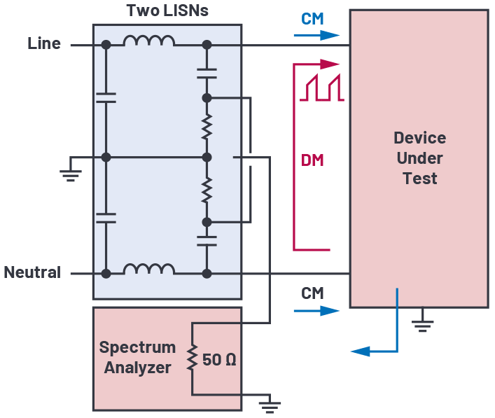
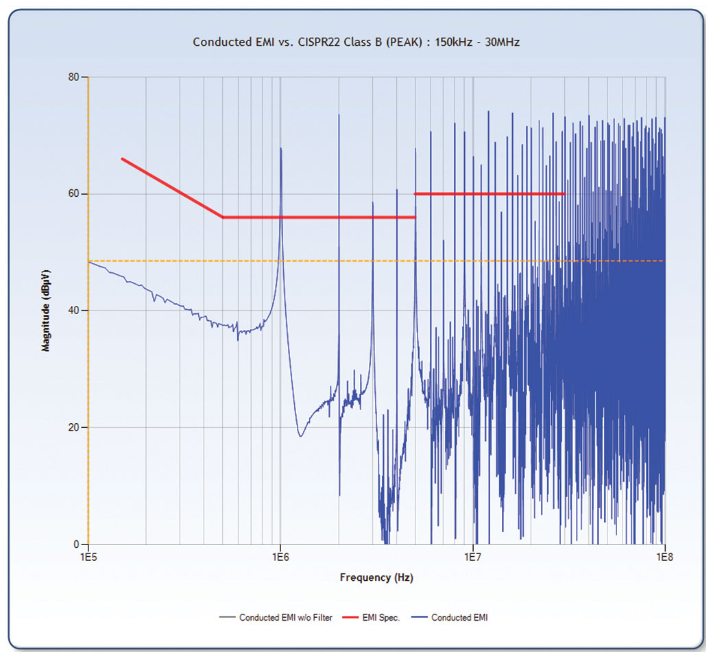
Figure 2 shows a typical EMI noise plot of a switch-mode, step-down buck supply without an input EMI filter. The most significant EMI spike occurs at the switching frequency of the supply, followed by additional spikes at its harmonic frequencies. Figure 2 shows an EMI plot where the peak values of these spikes exceed the CISPR 22 EMI limits. To meet the standard, an EMI filter is required to attenuate the differential-mode EMI.
Differential-Mode Conducted EMI Filter
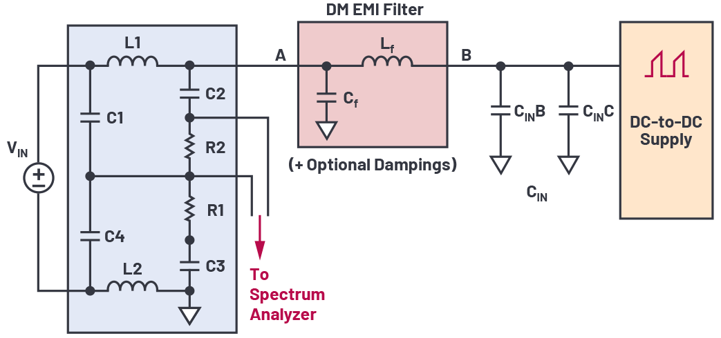
Figure 3 shows a typical differential-mode conducted EMI noise filter on the input side of a switch-mode supply. In this case, we’ve added a simple first-order, low-pass LfCf network between the supply’s local input capacitors CIN (EMI noise source side) and the input source (LISN receiver side). This matches a standard EMI lab test setup, where the LISN network is inserted on the filter capacitor Cf side of the LC filter. The differential signal across the LISN resistor R2 is measured by the spectrum analyzer to quantify DM conducted EMI noises.
Figure 4 shows the LC filter attenuation gain plot. At very low frequency, the inductor is low impedance, essentially shorted, while the capacitor is high impedance, essentially open circuit. The resulting LC filter gain is 1 (0 dB), allowing dc to pass through without attenuation. As frequency rises, a gain spike appears at the resonant frequency of LfCf. As the frequency rises above the resonant frequency, the filter attenuates at a rate of –40 dB/decade. At relatively higher frequencies, the filter gain increasingly becomes a function of parasitic components: namely, the filter capacitor’s ESR and ESL and filter inductor’s parallel capacitance.
Because this filter’s ability to attenuate quickly rises over frequency, the magnitude of first few low frequency noise harmonics overwhelmingly determine the size of the EMI filter—where the fundamental component of the supply’s switching frequency (fSW) is the most significant target. Therefore, we can focus on the EMI filter’s lower frequency gain in efforts to meet industry standards.
LTpowerCAD Can Predict Supply-Specific Filter Performance
LTpowerCAD is a power supply design assistance tool that can be downloaded at no charge at analog.com/LTpowerCAD. The program is designed to enable engineers to design and optimize complete power supply parameters in a few simple steps and in a few minutes.
LTpowerCAD leads a user through the entire power supply selection and design process, beginning with the user’s power supply specifications. From there, LTpowerCAD narrows the range of suitable solutions and then helps in the selection of power stage components, as well as optimizes supply efficiency, design loop compensation, and load transient response.
The feature we are interested in here is LTpowerCAD’s input EMI filter design tool, which enables an engineer to quickly estimate the differential-mode conducted EMI and determine what filter components may be required to meet EMI standards. LTpowerCAD’s filter tool can significantly reduce design time and cost by producing realistic results—before a single circuit board is built and tested.
EMI Filter Design in LTpowerCAD
Overview
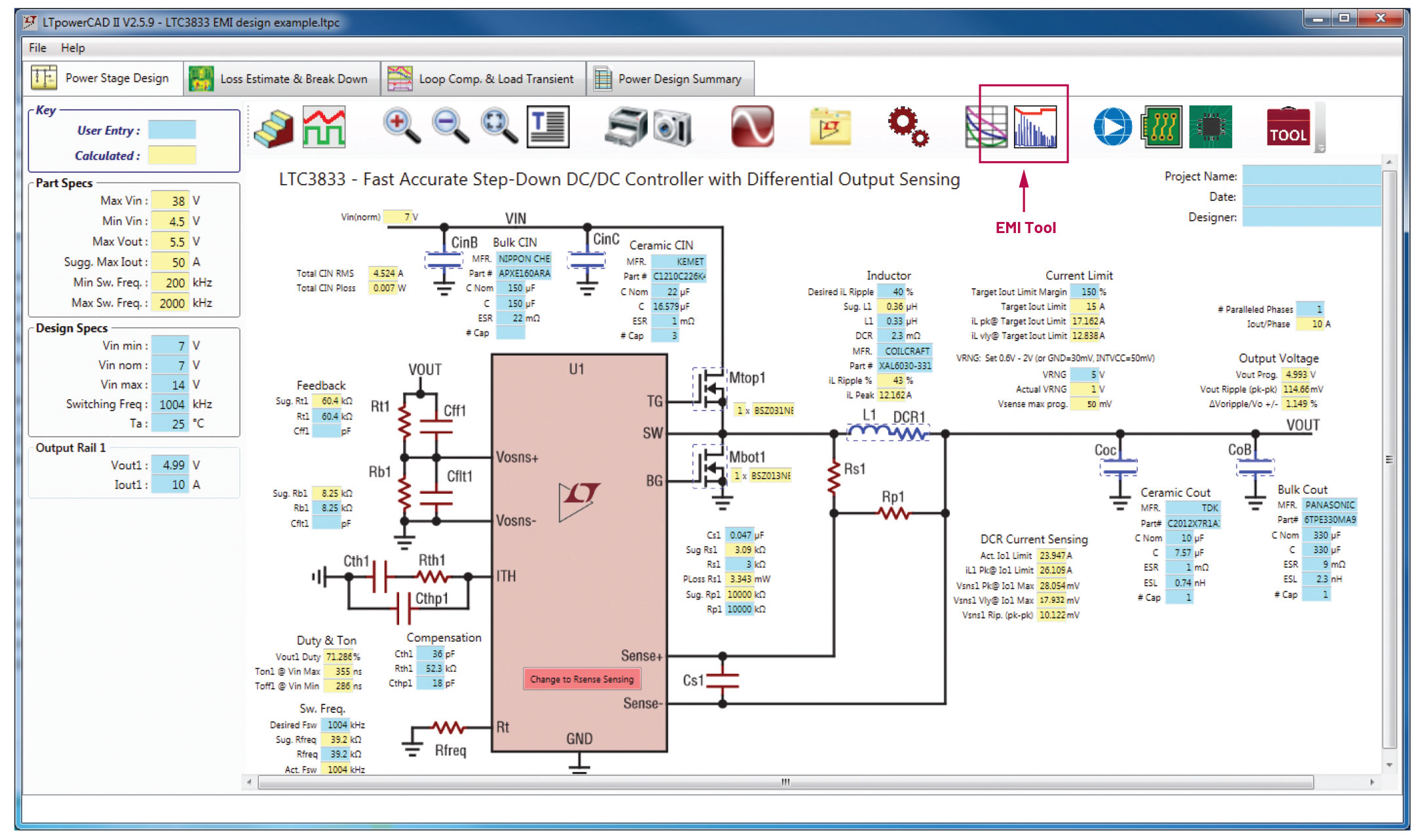
Let’s look at a DM EMI filter design example. Figure 5 shows the LTpowerCAD schematic design page, showing the component selection for a supply using the LTC3833 buck converter, operating with 12 V input and 5 V/10 A output, running at 1 MHz switching frequency, fSW. Before designing an EMI filter, design the buck converter by selecting the switching frequency, power stage inductor, capacitors, and FETs.
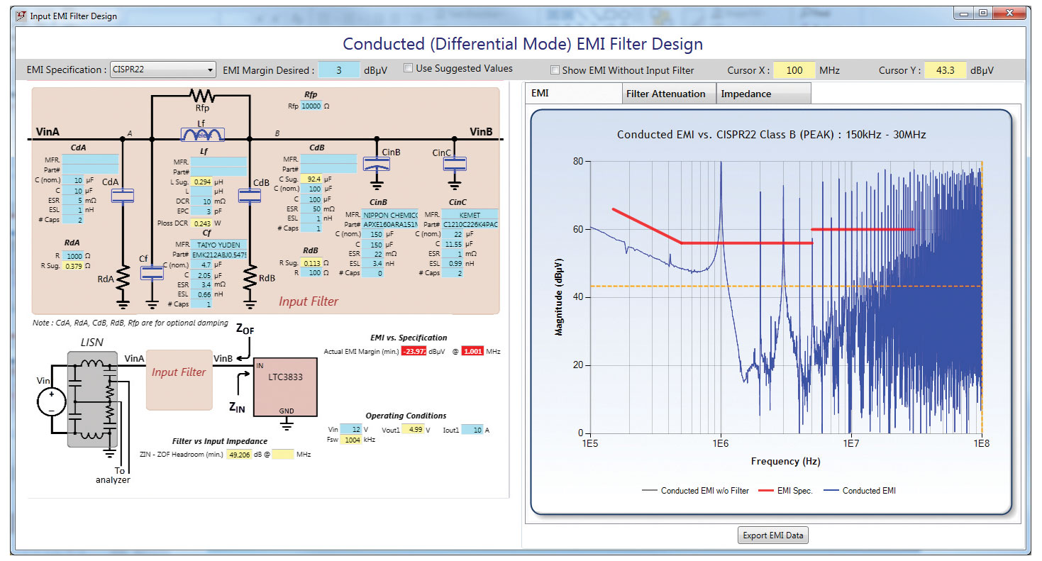
After power stage components are selected, click the EMI design icon to open the integrated DM EMI filter tool window, as shown in Figure 6. The EMI design window shows a detailed input filter network, LfCf, between the power supply input capacitors CINB/CINC and the source LISN. There are optional damping circuits, such as networks CdA/RdA on the LISN side, network CdB/RdB on the supply input capacitor side, and the optional damping resistor RfP across the filter inductor Lf. The estimated conducted EMI noise plot and the selected EMI standard limits appear on the right side of Figure 6.
Select an EMI standard
When designing an EMI filter, you’ll want to see the design’s targets—namely, the EMI standard itself. LTpowerCAD includes built-in plots for CISPR 22 (for IT equipment), CISPR 25 (for automotive devices), and MIL-STD-461G standards. Simply select your desired standard from the EMI Specification dropdown menu.
For example, in Figure 6, the filter inductor value is set at 0 to show the design’s EMI results without an input filter. EMI spikes at the fundamental and harmonic frequencies, all exceeding the displayed CISPR 25 limits, resulting in a red warning on the EMI vs. Specification schematic display.
Set the EMI Filter Parameters
After selecting the desired EMI standard, enter the desired EMI margin—what distance do you want between the selected standard limits and the peak values of the fundamental. A 3 dB to 6 dB margin is generally a good starting point. From these choices, for a given filter capacitor, Cf, and supply operating condition, the program calculates the suggested filter inductor value, L sug., shown in a yellow cell in LTpowerCAD. Enter an inductor value in the L cell slightly greater than the suggested value to meet the EMI limit with the desired margin.
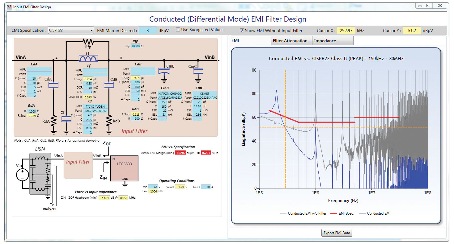
In this example, Figure 7 shows the design tool recommending a 0.669 µH filter inductance, along with the entered 0.72 µH inductance to meet the requirement. The benefits of the filter can be explored by comparing the results with and without the filter. Turn on the Show EMI Without Input Filter option to see the filtered results overlayed above a gray no-filter plot.
There is an important detail in choosing the filter capacitor Cf. If it is a multilayer ceramic capacitor (MLCC) with X5R, X7R, etc. type of dielectric material, its capacitance value can drop significantly with dc bias voltage. Because of this, in addition to the LTpowerCAD nominal capacitance, C(nom), the user should also enter its real capacitance under the applied dc bias voltage (VINA or VINB). The derating curve can be found from capacitor vendors’ data sheet. If the MLCC capacitor is chosen from the LTpowerCAD library, its derating with dc bias voltage is automatically estimated by the program.
Another component variation arises in the input filter inductor, which can have a nonlinear inductance due to its saturation with direct current. The inductance value may drop noticeably with increased load current, especially for a ferrite bead type of inductor. Users should enter the real inductance to produce accurate EMI predictions.
Check Filter Attenuation Gain
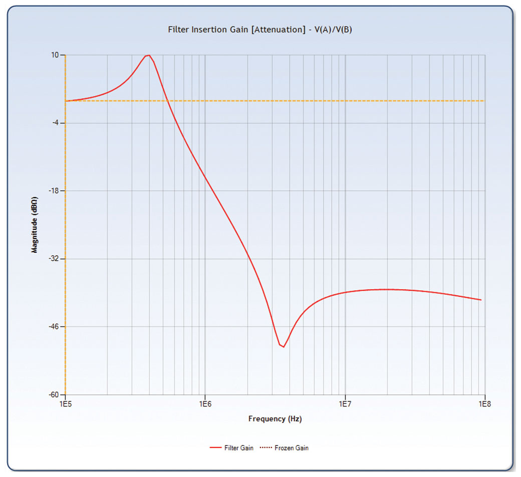
In the Figure 7 EMI plot with the input filter there is a noise spike due to the LC input filter resonance at 245 kHz, a frequency lower than the supply switching frequency. Figure 8 shows the filter attenuation gain plot in place of the EMI results in the LTpowerCAD EMI window (click the Filter Attenuation tab), revealing the filter’s resonant attenuation gain at 245 kHz.
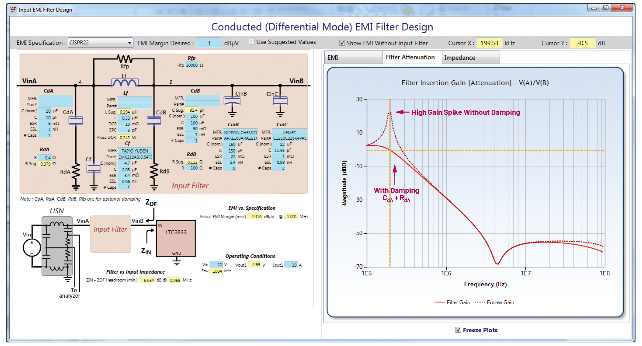
In some cases, the LC resonance peak can result in a spike that exceeds the EMI standard. To attenuate this resonant peak, a pair of optional damping components CdA and RdA can be added in parallel with the filter capacitor Cf. In addition to showing the attenuation plot, LTpowerCAD simplifies the selection process for these components. In general, choose a damping capacitance, CdA, that is around two to four times the real filter Cf value. LTpowerCAD will suggest a damping resistor RdA value to push down the resonant peak.
Check Filter Impedance and Supply Input Impedance
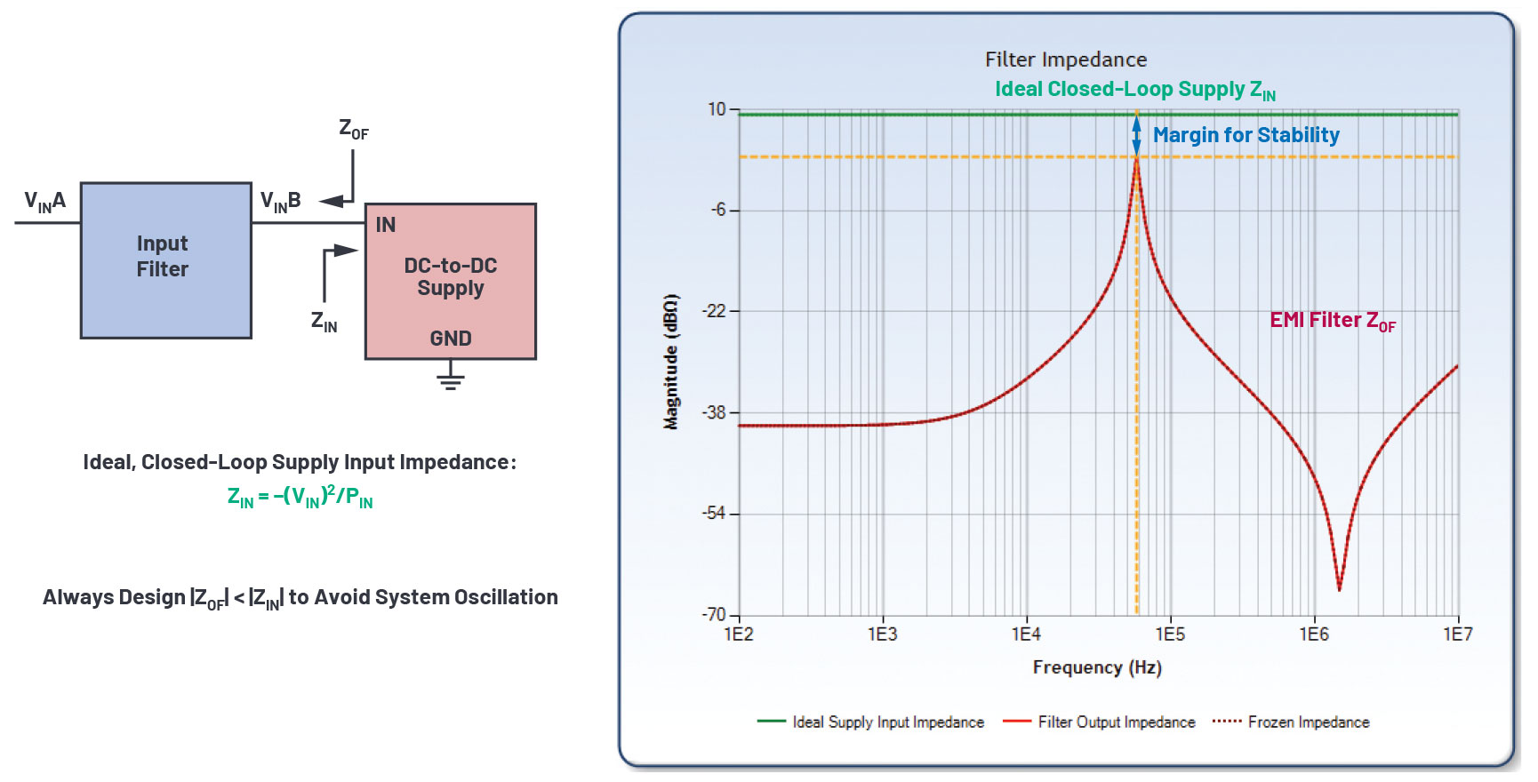
When adding an input EMI filter in front of a switch-mode supply, the filter output impedance, ZOF, can interact with the supply input impedance, ZIN, causing undesirable oscillation. To avoid this unstable situation, the magnitude of the EMI filter output impedance, ZOF, should be much lower than the magnitude of the supply input impedance, ZIN, with enough margin. Figure 9 shows the concept of ZOF and ZIN and the stability margin between them.
To simplify the problem, an ideal power supply with high feedback loop bandwidth can be treated as a constant power load; that is, input voltage VIN times input current is constant. As input voltage increases, its input current decreases. Therefore, the ideal power supply has a negative input impedance ZIN = –(VIN2)/PIN.
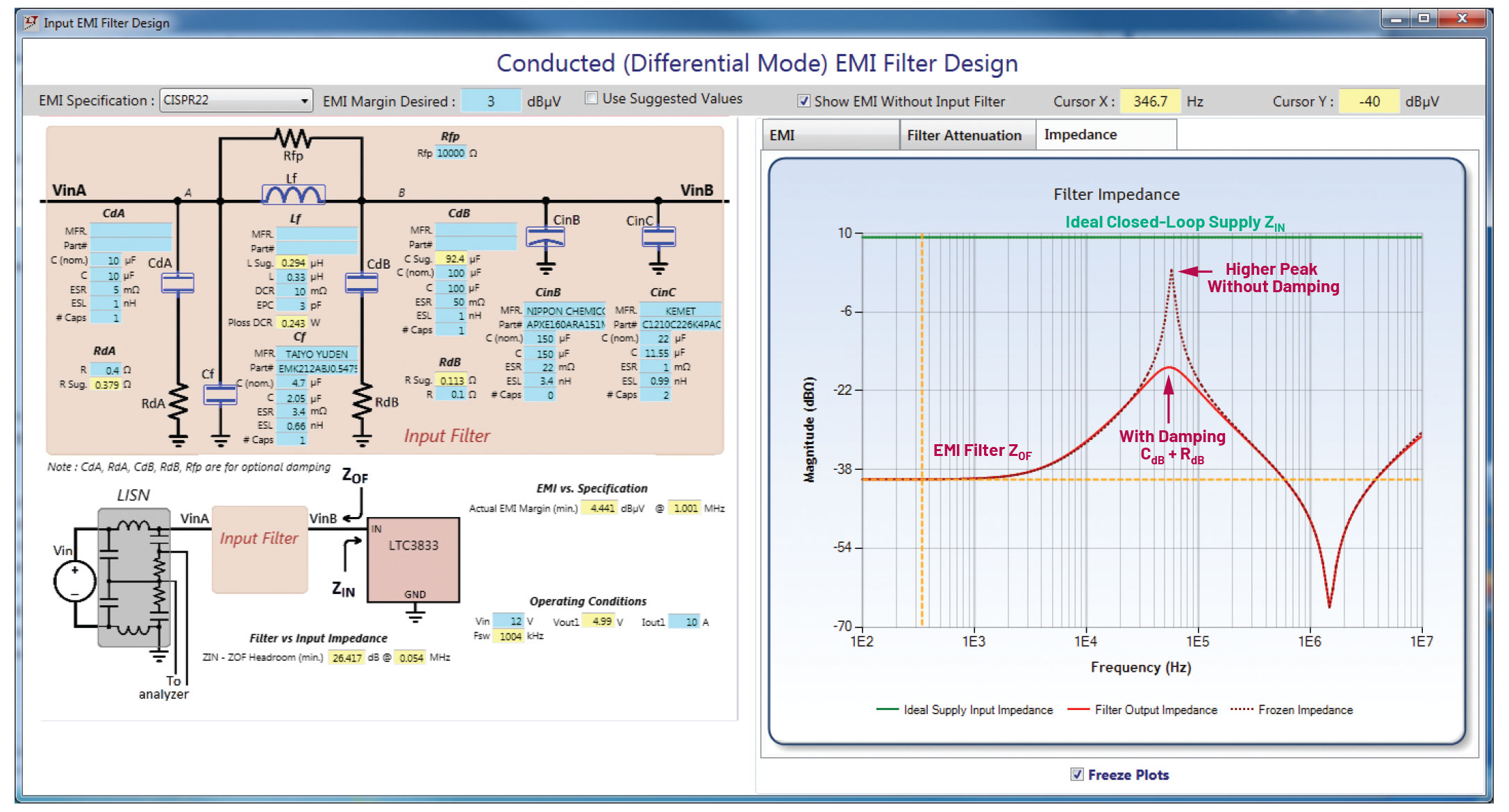
To make it easy to design the input filter, LTpowerCAD displays the filter output impedance ZOF and supply input impedance ZIN on the impedance plot shown in Figure 10. Note the supply input impedance is a function of input voltage and input power. The worst case, which is the lowest level of impedance, occurs at the minimum VIN and maximum PIN condition.
As shown in Figure 10, the EMI filter output impedance has a peak point at the resonant frequency caused by filter inductor Lf and supply input capacitor CIN. In a good design, the magnitude of this peak should be lower than worst-case ZIN, with enough margin. In case it is necessary reduce this peak level, there is another pair of optional damping components, capacitor CdB and resistor RdB, in parallel with the supply input capacitor CIN. This CIN side damping network can effectively reduce the ZOUT peak. The suggested CdB and RdB values are provided by LTpowerCAD EMI tool.
Accuracy of the LTpowerCAD EMI filter tool
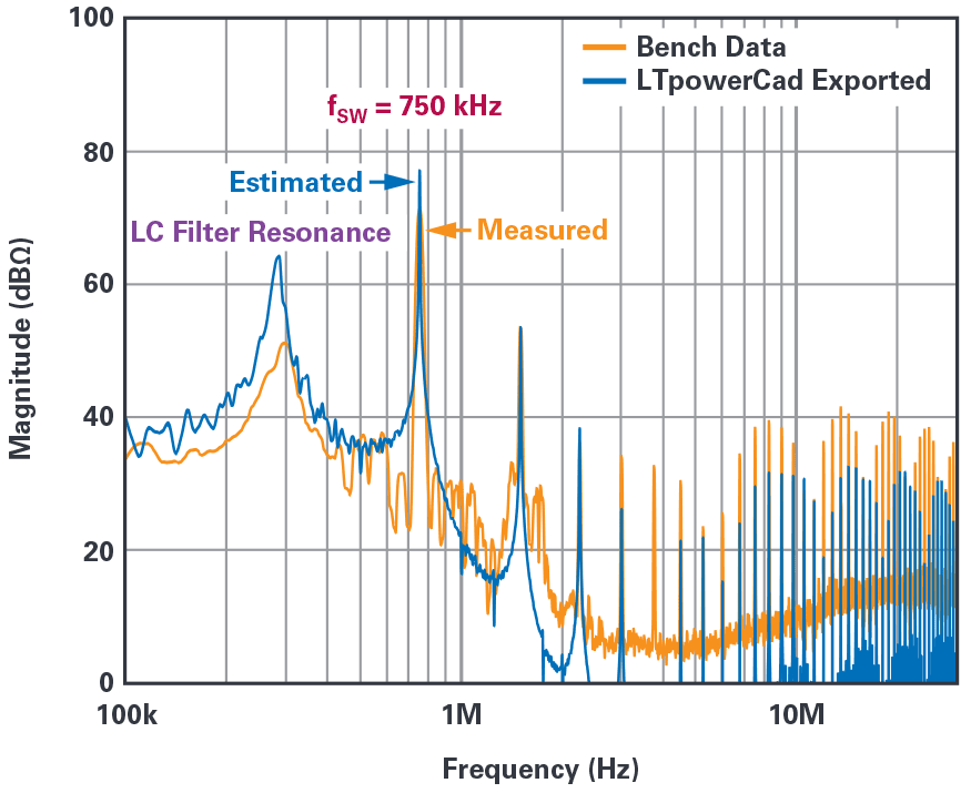
The accuracy of the LTpowerCAD EMI filter tool can be seen by running an LTpowerCAD design against a real board, lab EMI test. Figure 11 shows the results of a comparison where the real-world test was performed using a modified LTC3851 buck supply demo board running at 750 kHz with a 12 V input voltage, 1.5 V output voltage, and 10 A load current. As shown in Figure 11, tested EMI data and LTpowerCAD modeled EMI data match well for lower frequency noise peaks, while real-world tested peaks are a few dB lower than modeled EMI peaks.
There are larger mismatches at higher frequency noise peaks, but these are of lower importance because the DM conducted EMI filter size is mainly determined by lower frequency noise spikes. Some of this discrepancy is due to the accuracy of inductor and capacitor parasitic models, including PCB layout parasitic values; accuracy that is beyond what is possible in a PC-based design tool, for now.
Please note the LTpowerCAD filter tool is an estimation tool, providing an initial design point for EMI filters. Nothing can replace a real lab test of a prototype supply board for truly accurate EMI data.
Summary
Many industries are using systems that require increasingly careful control of transmitted electromagnetic signals. To this end, there are a number of published clear standards on EMI. At the same time, the number of switch-mode power supplies is increasing, and they are being placed ever closer in proximity to sensitive circuits. Switch-mode power supplies are strong sources of EMI, so their noise output must be quantified and reduced in many cases. The problem is, EMI filter design and testing is a time-consuming and costly iterative process.
LTpowerCAD enables designers to save time and cost by precluding real-world design and test with predictive computer-based design tools. Its easy to use EMI filter tool predicts the results of differential-mode conducted EMI filters, including optional damping networks, to minimize EMI while retaining a stable supply. Lab test results verify the accuracy of predictive models.


