ADGS1612相关信息来自ADI官网,详细参数以官网发布为准,ADGS1612供给信息可在查IC网查找相关供给商。
产品概况
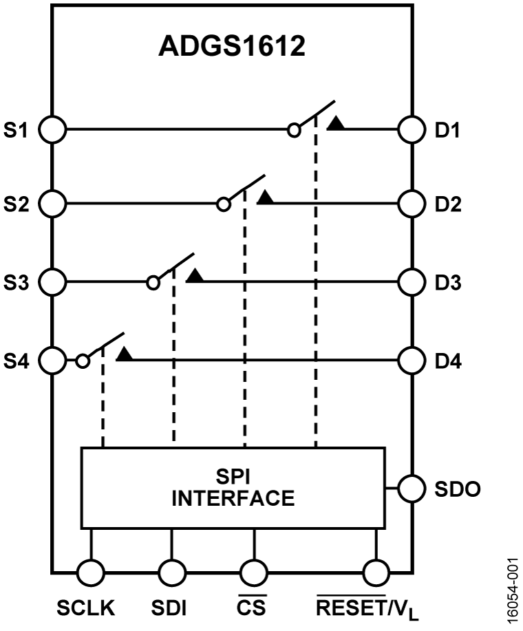
The ADGS1612 contains four independent single-pole/single-throw (SPST) switches. A serial peripheral interface (SPI) controls the switches. The SPI interface has robust error detection features, including cyclic redundancy check (CRC) error detection, invalid read/write address detection, and serial clock (SCLK)count error detection.
It is possible to daisy-chain multiple ADGS1612 devices together. Daisy-chaining enables the configuration of multiple devices with a minimal amount of digital lines. The ADGS1612 can also operate in burst mode to decrease the time between SPI commands.
Each switch conducts equally well in both directions when on, and each switch has an input signal range that extends to the supplies. In the off condition, signal levels up to the supplies are blocked.
The ultralow on resistance (RON) of these switches make them ideal solutions for data acquisition and gain switchingapplications where low RON and low distortion are critical. The RON profile is very flat over the full analog input range, ensuring excellent linearity and low distortion when switching audio signals. The ADGS1612 exhibits break-before-make switchingaction for use in multiplexer applications. Note that throughout this data sheet, the multifunction pin, RESET/VL, is referred to either by the entire pin name or by a single function of the pin,for example, VL, when only that function is relevant.
Product Highlight
- The SPI interface removes the need for parallel conversion and logic traces and reduces general-purpose input/output (GPIO) channel count.
- Daisy-chain mode removes additional logic traces when multiple devices are used.
- CRC, invalid read/write address, and SCLK count error detection ensure a robust digital interface.
- CRC error detection capabilities allow the use of the ADGS1612 in safety critical systems.
- Guaranteed break-before-make switching allows the use of the ADGS1612 in multiplexer configurations with external wiring.
- Minimum distortion.
Applications
- Communication systems
- Medical systems
- Audio and video signal routing
- Automatic test equipment
- Data acquisition systems
- Battery-powered systems
- Sample-and-hold systems
- Relay replacements
优势和特色
- SPI interface with error detection
- Includes CRC, invalid read/write address, and SCLK count error detection
- Supports burst mode and daisy-chain mode
- Industry-standard SPI Mode 0 and SPI Mode 3 interface compatible
- Guaranteed break-before-make switching allowing external wiring of switches to deliver multiplexer configurations
- 1 Ω typical on resistance at 25°C
- 0.23 Ω typical on resistance flatness at 25°C
- VSS to VDD analog signal range
- Fully specified at ±5 V, 12 V, 5 V, and 3.3 V
- ±3.3 V to ±8 V dual-supply operation
- 3.3 V to 16 V single-supply operation
- 1.8 V logic compatibility with 2.7 V ≤ VL ≤ 3.3 V
- 4 mm × 4 mm, 24-lead LFCSP package
ADGS1612电路图
ADGS1612中文PDF下载地址
ADGS1612下载链接地址:https://www.analog.com/media/cn/technical-documentation/data-sheets/adgs1612_cn.pdf